Solid and Semiconductor
The material having conductivity between the conductor and insulator is called a semiconductor.
- The conductivity of semiconductors increases with increases in temperature.
- At low temperatures, their conductivity is very small and behaves like insulators.
- At high temperatures, they behave like conductors. –
- Rθ = Ro (1- αT); variation of resistance with temperature. –
- The resistance decreases with an increase in temperature.
- Examples: Germanium (Ge), Silicon (Si), Carbon (C), etc. –
- They have 4 electrons in the outermost shell.
Intrinsic and Extrinsic Semiconductor Intrinsic Semiconductor: – - The semiconductor found in pure form are called intrinsic semiconductors – Ge, Si, etc. –
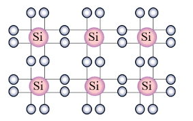
- They share the electrons with the nearest 4 neighbor atoms. –
- Due to an increase in temperature, the electron can break the covalent bonds as a result it is emitted from the atom.
- The vacancy of an electron is called the hole. A hole is considered opposite the charge of an electron.
- Electrons exist in the conduction band and holes exist in the valance band.
Extrinsic Semi-Conductor
- An intrinsic semiconductor mixed with a suitable impurity atom is called an extrinsic
- semiconductor. They are two types of extrinsic semiconductors: P type and N type.
| S.N | P-Type | N-Type |
| 1 | Intrinsic semiconductor doping with a trivalent impurity atom gives a P-type semiconductor. | Intrinsic semiconductor doping with pentavalent impurity atom gives P-type semiconductors. |
| 2 | Trivalent impurities are Aluminum, Indium, Boron, Gallium, etc. | Pentavalent impurity: Phosphrous, Antimony, Arsenic, etc |
| 3 | They have excess free holes in comparison to free electrons. | They have an excess of free electrons in comparison to free holes. |
| 4 | The impurity atom is called the acceptor. | The impurity atom is called a doner. |

PN Junction Diodes:
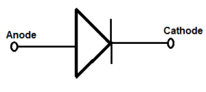
It is a semiconductor device made by joining two different types of extrinsic semiconductors. Its one-half section is p-type, and another half is n-type. Therefore, it is called a PN junction diode. The two ends are acting as two terminals. Therefore, it is called
a diode.
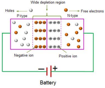
The layer at which the different types of semiconductor meet is called a junction. The junction acts as a boundary wall between the p and n sides.
When the p-n junction diode is made, in a small region near the junction the holes from p-type and electrons from n-type cross the junction, i.e., the majority charge carrier from each side crosses the junction.
As a result, the small region towards the p-type material is depleted with holes, and the small region towards the n-type material is depleted with electrons. The majority of charge carrier from each side crosses the junction. The region near the junction in which the majority charge carrier is depleted is called the depletion region/layer. In the depletion region, the opposite nature of charge occupies each part.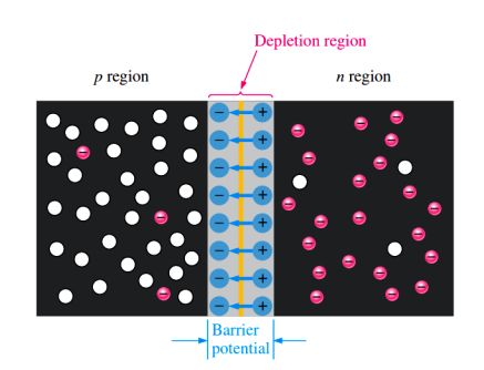
Barrier Potential:
The depleted charges create a potential difference in the depletion region. This potential difference is called barrier potential. The majority of charges can cross the junction if the applied potential is greater than the barrier potential.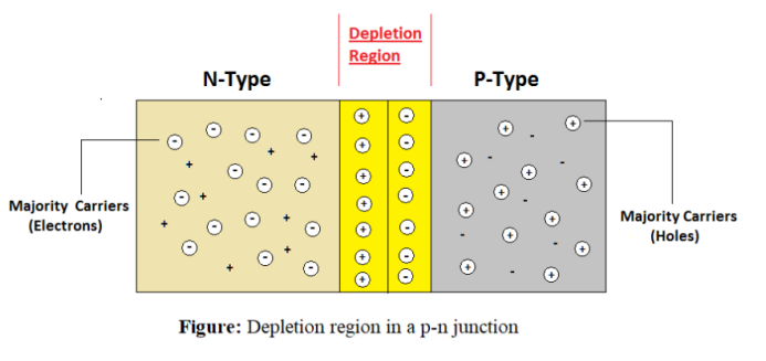
Biasing of PN junction diode:
The technique of connecting DC voltage or supplying DC current to the desired level for the proper flow of AC signal within the p-n junction is called biasing. Biasing helps to work properly. We can connect the p-n junction diode with the DC source in two ways.
Accordingly, there are two types of biasing.
- Forward Biasing:
- Reverse Biasing
Forward Biasing:
If the p-type region is connected towards the positive terminal and the n-type region is connected towards the negative terminal of the DC voltage source, then it is called forward bias. The applied voltage mostly drops across the depletion region and the voltage drop across the p-side and n-side of the junction is negligible. This is because the resistance of the depletion region is very high compared to the resistance of the n-side and p-side. The direction of the applied voltage is opposite to the barrier potential. As a result, the depletion layer width decreases.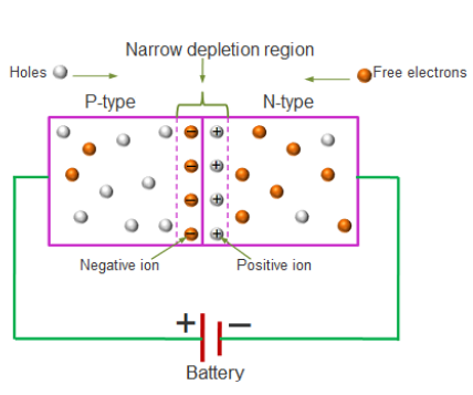
Reverse Biasing:
When an external voltage (V) is applied across the diode such that the n-side is connected to the positive terminal of the battery and the p-side is connected to the negative terminal of a battery, it is said to be reverse biased The applied voltage mostly drops across the depletion region. The direction of the applied voltage is the same as the direction of barrier potential. As a result, the width of the depletion region increases due to the movement of the majority of charges away from a junction. The majority of charges can’t cross the junction as a result there is no current due to the flow of the majority of charges. But the minority charges get forward biased. They cross the junction. The number of minority charges is very less, therefore the current due to flow of minority charges is very small. This is called reversed current or minority current.