
 by
by The process of applying the external DC voltage to a p-n junction semiconductor diode is called biasing. To make the current flow, it is necessary to “bias” the diode.
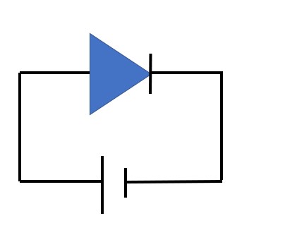
>Forward biased diode
A forward bias condition is established by applying the positive potential to the P-type material and the negative voltage potential to N-type material.
A diode acts as a semiconductor hence no more voltage drop across the diode and a large forward current flow through the diode.
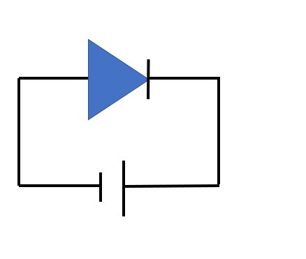
>Reverse biased diode
A reverse bias condition is established by applying the positive potential to the N-type material and the negative potential to the P-type material.
In reverse bias condition a small current flow through the diode called reverse saturation current, due to the movement of minority carriers.
>If this reverse applied voltage continuously increases after a certain reverse applied voltage a large reverse current flow through the device and the depletion region will be destroyed .
>If the reverse current is not limited by an external resistance, it will destroy the diode.
Application
Diode work like a switch.
Diode work as a Rectifier.
can we use transistor as a switch to make wireless electornic device
Yes you can used transistor as switch to make wireless electronic device because we know transistor does not conduct through it in cut off region(voltage below threshold) and fully conduct in saturation region(voltage above threshold)