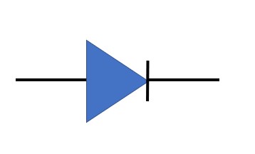
>The term “di-ode” means having “two-electrode” and it is a semiconductor device having two terminal “anode and cathode” that conduct current in only one direction.

>An ideal diode will have zero resistance in the forward bias direction & infinite resistance in the reverse bias direction.
>It works like a switch.
Formation of diode
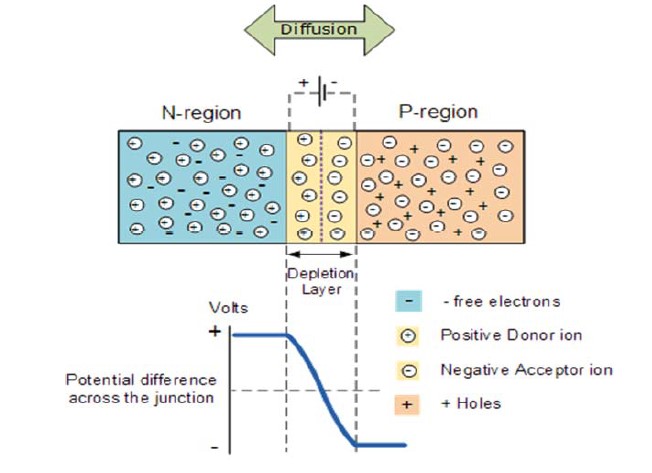
>When a P-type semiconductor is suitably joined with an N-type semiconductor, a junction is formed called P-N junction, and the device formed is called P-N junction diode.
During the formation of the P-N junction, the following two phenomena take place.
- A thin deplection layer (or region) is set up on both side of junction and is so called because it is depleted or devoid of free charge carriers. Its widht is about 1μm.
- A junction or barrier potential Vb is develop across the junction whose value is about 0.3V for Ge and 0.7V for Si. When P-N junction is packed as semiconductor device, it is called P-N junction diode.

>The semiconductor material used for diodes such as silicon, germanium, and arsenide.
>For designing diodes, silicon is more preferred over germanium because silicon semiconductor -works at a higher temperature compared with germanium diode.
>In n-type semiconductors, free electrons are the majority charge carriers whereas, in p-type semiconductors, holes are the majority charge carriers.
>
